Security testing of the pacemaker ecosystem - Part 2
Hardware testing of the Home Monitoring Unit Link to heading
When I first started to work on that project, I had very little knowledge about hardware security and hardware in general. However, working on this topic was a challenge, and I learned a lot along the process. The target was the Cardio Messenger IIS Home Monitoring Unit manufactured by BIOTRONIK, a German company. I had no real idea what to begin with, but it seemed that looking for the debug ports was the way to go. Thus, this post will focus on locating the debug ports and on extracting the firmware out of the HMU.
Looking for debug ports Link to heading
Components identification Link to heading
First thing first, I opened the device to see what kind of hardware I was facing. The goal at this stage is to identify the main (active) components on the board and to construct a simple schematic with the interactions between those. Figure 1 presents the CardioMessenger II-S in its Telephone Line version. The GSM version is very similar, and only the modem changes. This is why, this post will mainly use pictures of the T-Line as it is the device I performed my initial testing on. However, all findings were verified later on the GSM version as well.
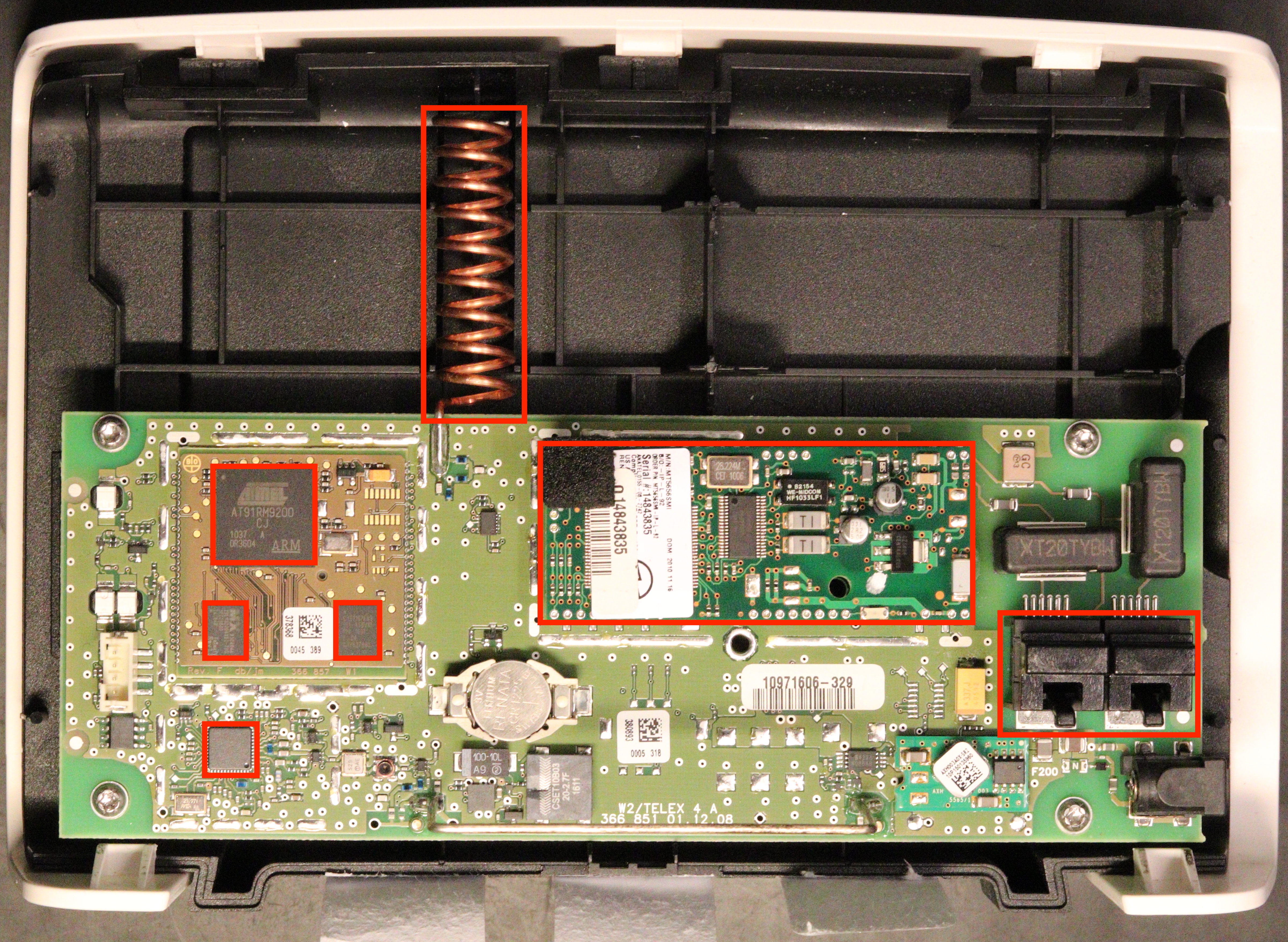
Figure 1: Inside of the CardioMessenger II-S T-Line
I started by looking up online for the datasheets from the different parts on the PCB. It is interesting to notice that the PCB can be devided in three distinct parts:
- The main PCB
- “The microcontroller PCB”, which is in the upper left square
- The modem (which is plugged into the main PCB and can be removed on the T-LINE version)
On the microcontroller PCB, there are:
- the microcontroller, an AT91RM9200 from Atmel (now microchip)
- a 4Mb Burst flash memory
- an external RAM
Looking at what remain on the PCB, there is Digital Signal Processor (bottom left corner on Figure 1) and a modem. We can draw the very simple schematic presented in Figure 2.
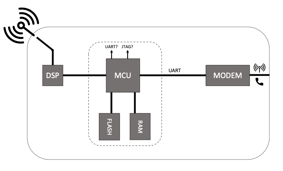
Figure 2: HMU Schematic
Having this schematic makes it clear where we can do some testing. In this project, I tested mainly on the debug ports (UART/JTAG) and on the communication between MCU and Modem. However, one could also have tried to interact directly with the flash if the proper equipment is available.
Before starting the work on the CardioMessenger II-S, I analyzed other medical devices that were known to have vulnerabilities, such as the Merlin@Home from St Jude Medical or an old HMU from Medtronic. The Merlin@Home was an embedded Linux system, and getting access to it was pretty straight forward: once connected to the device via UART (labelled), you are prompted to log in. However, if you interrupt the boot, you get a terminl in the Blob Bootloader, with some available commands. Issuing the boot init=/bin/sh command with the proper arguments gives you a shell as root. As simple as that.
I was then wondering if I could be facing something similar with the CardioMessenger II-S, but when looking at the components, even though it could have been feasible, I had a hard time to believe it could be an embedded Linux running on the HMU, and thus made the assumption that it was some custom OS built on top of famous real-time OS, like Free RTOS for instance.
So, the next thing to do was to look for the debug ports on the board. We learn from the datasheet of the MCU that JTAG/SWD and UART are available. Looking more closely at the PCB part around the microcontroller, we can identify several points of interest. They are presented in red on Figure 3.
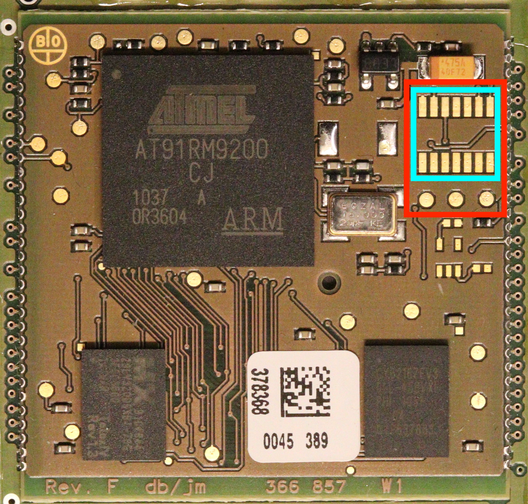
Figure 3: Possible debug ports on the board
Looking for the UART Link to heading
Main UART Link to heading
The pins were not labelled on the device, so the steps I took to figure out which correspond to the UART were:
- Determining the ground pin using a multimeter and a known ground reference (metal parts of the device can do the trick if nothing better is available). Having a continuity test functioanlity available comes quite handy here.
- To prevent hooking up my computer to a random couple of pins and pray for it to work, I then used an oscilloscope to monitor what was happening on the different pins during boot. Activity, if any, can be detected on TX.
- Lastly, we need the Baud rate that is used. One solution could be to simply hook up the computer and try different ones until we get something that makes sense. However, a better way is to used an oscilloscope (or logic analyzer) to determine the bit period, and then take its inverse to get the Baud rate.
Coming back to the HMU, the 3 pins below the ones highlighted in cyan in Figure 3 corresponds to ones of the UART. When looking at what is sent on the TX pin during boot, I got the following output:
Bootloader TELEX4:but nothing more. I tried looking up for this string online but did not get any relevant information out of it. It confirmed I have indeed found the UART. It also seems like no debug information is sent to it.
I then tried to see if I could interact with it, and sent to issue keystrokes such as “ENTER”, “CTRL+C”, “ESC”, etc. but did not get any interaction. The text is not echoed either.
Communication between the microcontroller and the modem Link to heading
UART is not only used to output debug information, but also to communicate between two components as it can be seen from the schematic presented in Figure 2. Here, it is used by the modem and the microcontroller to communicate together. When looking online for the datasheet of the modem, we easily find the UART pins of the modem. We do not want to send anything here for now, only eavesdrop the communication. For that we can hook up the TX pin of the modem (which correspond to its “input” according to the doc) to the RX pin of the USB-to-TLL to get the communication from the microcontroller to the modem. We can do the same with RX, connected to the RX pin of another USB-to-TTL to get the communication from the modem to the microcontroller. From there we can observe an interesting communication taking place:
[2019-03-30 11:43:24] at
atii5#vversion
AT#MCOUNTRY?
at
AT+WOPEN=1
AT#DIALSELECT=1
AT#AUTHENT=PAP
at#atcmd=0,"-STE=7"
at#atcmd=1,"+A8E=6,5,0,1,0,0"
at#atcmd=2,"X3"
at
AT#DIALN1="T9W[REDACTED]"
AT#ISPUN="[REDACTED]@cm3-homemonitoring.de"
AT#ISPPW="[REDACTED]"
at#atcmd=0,"-STE=7"
[2019-03-30 11:43:26] AT#CONNECTIONSTART
[2019-03-30 11:43:28] at#connectionstop
As can be observed, the microcontroller is configuring the modem using AT commands. By looking at the “AT Commands for GSM/GPRS Wireless Modems with IP Connectivity”, we learn that the modem is ordered by the microcontroller to connect to an Access Point Name (APN), which is the gateway between the mobile network and another network, usually the internet. Firstly, it starts the TCP/IP stack with the WOPEN command and then, selects the primary Dial number to be used with the DIALSELECT command. The authentication method is then set to Password Authentication Protocol (PAP). Finally, the dial number is set, along with the username and password required to connect to the APN (ISPUN and ISPPW commands). Username and password are sent in clear text. Also, we noticed that the username corresponds to the serial number of the device, which is printed on a label below it. I will come back to those credentials in the last post of this series, and which role they play in the full attack scenario. This interface will also be studied more in depth in the next post.
Looking for JTAG Link to heading
Another common way to compromise an IoT device is to use the JTAG interface. In the case of the CardioMessenger II-S, the JTAG pins were not labelled either and there were several candidates: the 14 pins framed in cyan in Figure 2. However, only 5 pins are required for JTAG. I did not have the proper equipment to probe all 14 pins at the same time, and thanks to an engineer from the NTNU’s Electronic Department (thanks again Ingulf if you happen to read this), we were able to add a proper connector onto those pins. Figure 4 presents the connector that has been added along with the soldering performed on the board.
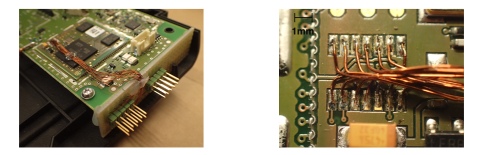
Figure 4: Details of the connector added to the board
Identification of the JTAG pins Link to heading
To determine the pinout of the JTAG interface, we used a special hardware tool called “JTAGulator”. As explain by Grand Idea Studio, the distributer of the JTAGulator, it is an “open source hardware tool that assists in identifying OCD connections from test points, vias, or component pads on a target device.” Basically, it can guess the pinout of the JTAG interface by trying all possible permutations. The JTAGulator is an inexpensive commercial off-the-shelf equipment and is presented in Figure 5.
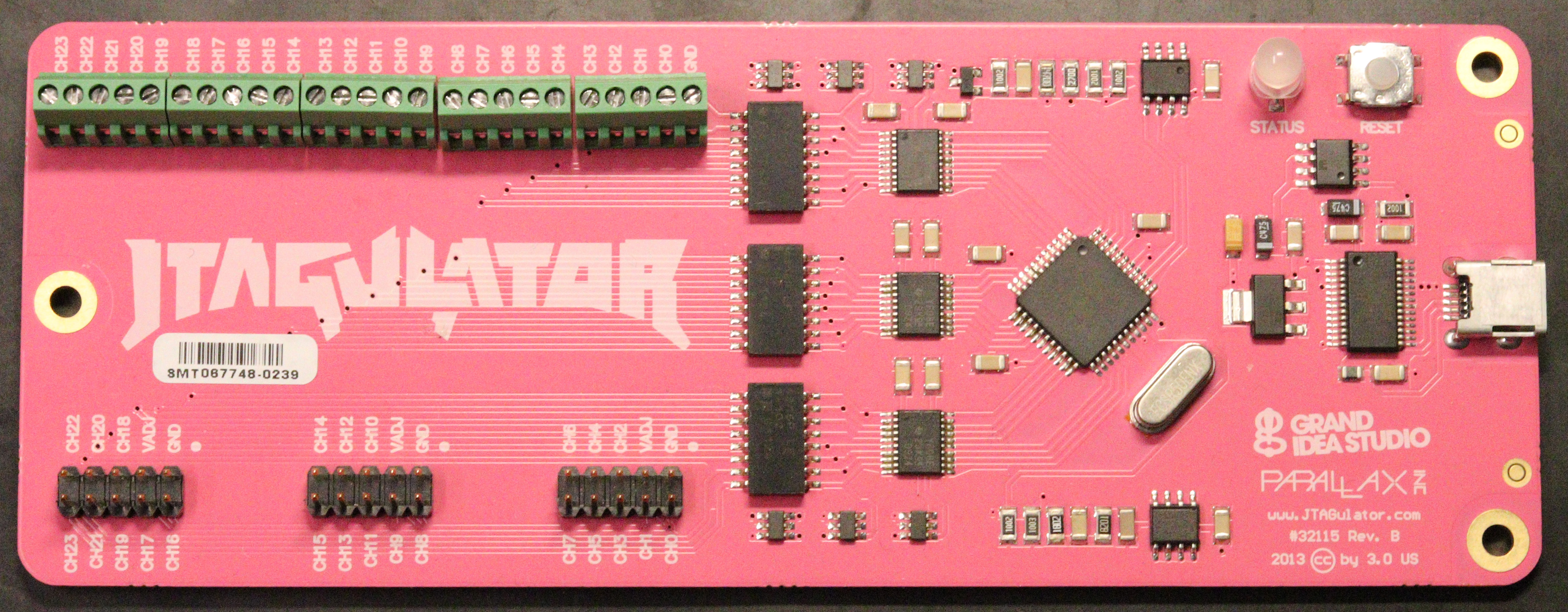
Figure 5: The JTAGulator from Grand Idea Studio
The device is easy to use. First, we need to connect the interesting pins of the board to the JTAGulator (as presented in Figure 6). The JTAGulator is then connected to the computer with USB and one can interact with it through screen for instance. The Baud rate is 115 200 Bd/s.
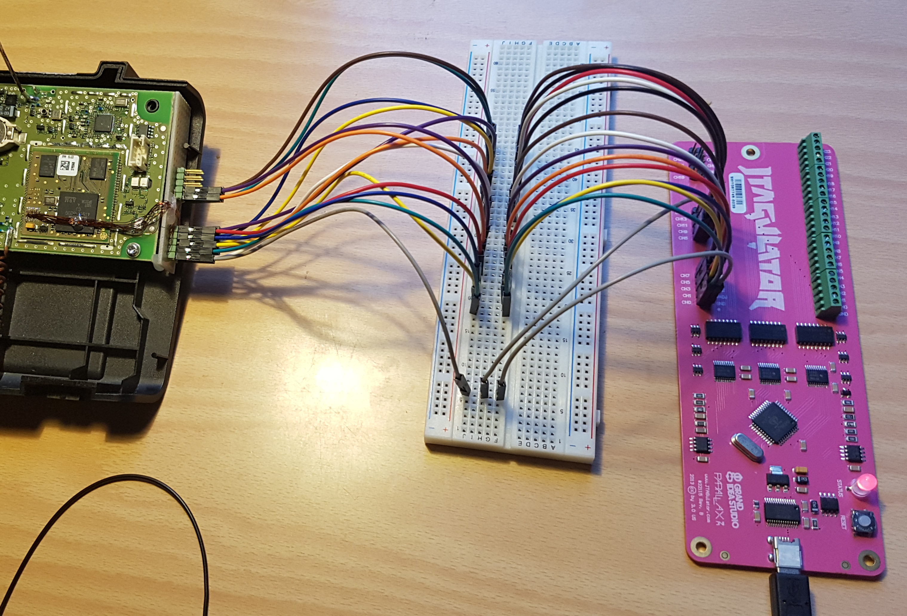
Figure 6: The JTAGulator connected to the device
Once the device connected, the steps are the following:
-
Adjust the voltage of the JTAGulator (3.3V in the case of the CardioMessenger II-S)
-
Launch an IDCODE scan to determine TDO, TMS, TCK, TRST
JTAG> i Enter starting channel [0]: Enter ending channel [0]: 12 Possible permutations: 1716 Bring channels LOW between each permutation? [y/N]: y Enter length of time for channels to remain LOW (in ms, 1 - 1000) [100]: Enter length of time after channels return HIGH before proceeding (in ms, 1 - 1000) [100]: Press spacebar to begin (any other key to abort)... JTAGulating! Press any key to abort... ------------------------------------------- TDI: N/A TDO: 11 TCK: 4 TMS: 12 Device ID #1: 0000 0101101100000010 00000011111 1 (0x05B0203F) TRST #: 3 TRST #: 10 ------------------------------------------- IDCODE scan complete. -
Launch a BYPASS scan to get TDI
JTAG> b Enter starting channel [0]: Enter ending channel [12]: Are any pins already known? [Y/n]: y Enter X for any unknown pin. Enter TDI pin [0]: x Enter TDO pin [11]: Enter TCK pin [4]: Enter TMS pin [12]: Possible permutations: 10 Bring channels LOW between each permutation? [Y/n]: y Enter length of time for channels to remain LOW (in ms, 1 - 1000) [100]: Enter length of time after channels return HIGH before proceeding (in ms, 1 - 1000) [100]: Press spacebar to begin (any other key to abort)... JTAGulating! Press any key to abort... ---- TDI: 5 TDO: 11 TCK: 4 TMS: 12 TRST #: TRST #: Number of devices detected: 1 ------ BYPASS scan complete. -
Read the device ID to confirm the pinout
JTAG> d
TDI not needed to retrieve Device ID.
Enter TDO pin [11]:
Enter TCK pin [4]:
Enter TMS pin [12]:
Device ID #1: 0000 0101101100000010 00000011111 1 (0 x05B0203F)
-> Manufacturer ID: 0x01F -> Part Number: 0x5B02
-> Version: 0x0
IDCODE listing complete.
The JTAG pinout is then:
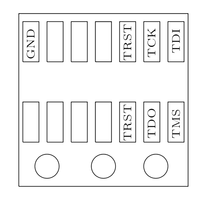
Figure 7: JTAG pinout on the CardioMessenger II-S
Firmware extraction Link to heading
Great! Now that we have the JTAG pinout, we can connect a JTAG adapter and start interacting with the microcontroller to get what we are really looking for here: the firmware. In my case, I used a Raspberry Pi Zero as presented in Figure 8. My goal was to use only COTS equipment and open-source software, trying to get the cost as low as possible.
Establishing the connection with OpenOCD Link to heading
OpenOCD (Open On-Chip-Debugger) aims at providing debugging, in-system programming and boundary-scan testing for embedded target devices as explained by Dominic Rath in its PhD Thesis. Used along with a small adapter which provides the user with the required electrical signals, we can perform on-chip-debugging or programming without the need of an external, and often expensive, programmer. As mentioned above, it can be used with a Raspberry Pi Zero, which costs around $10. Another cheap alternative to the Raspberry Pi Zero is The Shikra developed by Xipiter. The drawback of using OpenOCD is that it can be unstable or contain bug. Furthermore, it is not necessarily straight forward to understand when used for the first time. Despite of this, it becomes a very powerful tool once the configuration’s problems are solved. I really like the ability to write configs for OpenOCD, which can be used almost like “scripts.”
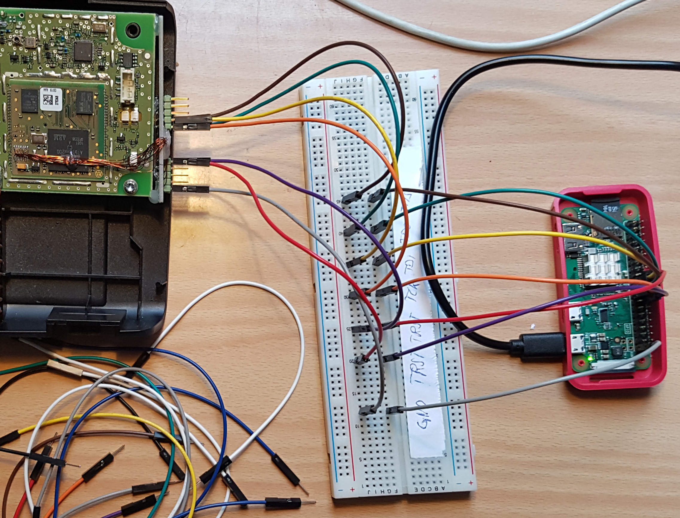
Figure 8: Using a Raspberry Pi Zero as JTAG adapter
Once connected to the device, we can simply ssh to the RasperryPi and test the connection. First we need to start OpenOCD, issuing sudo openocd -f your_config.cfg, then we connect to it issuing nc 127.0.0.1 4444, and then issue the scan_chain command to detect what devices are present.
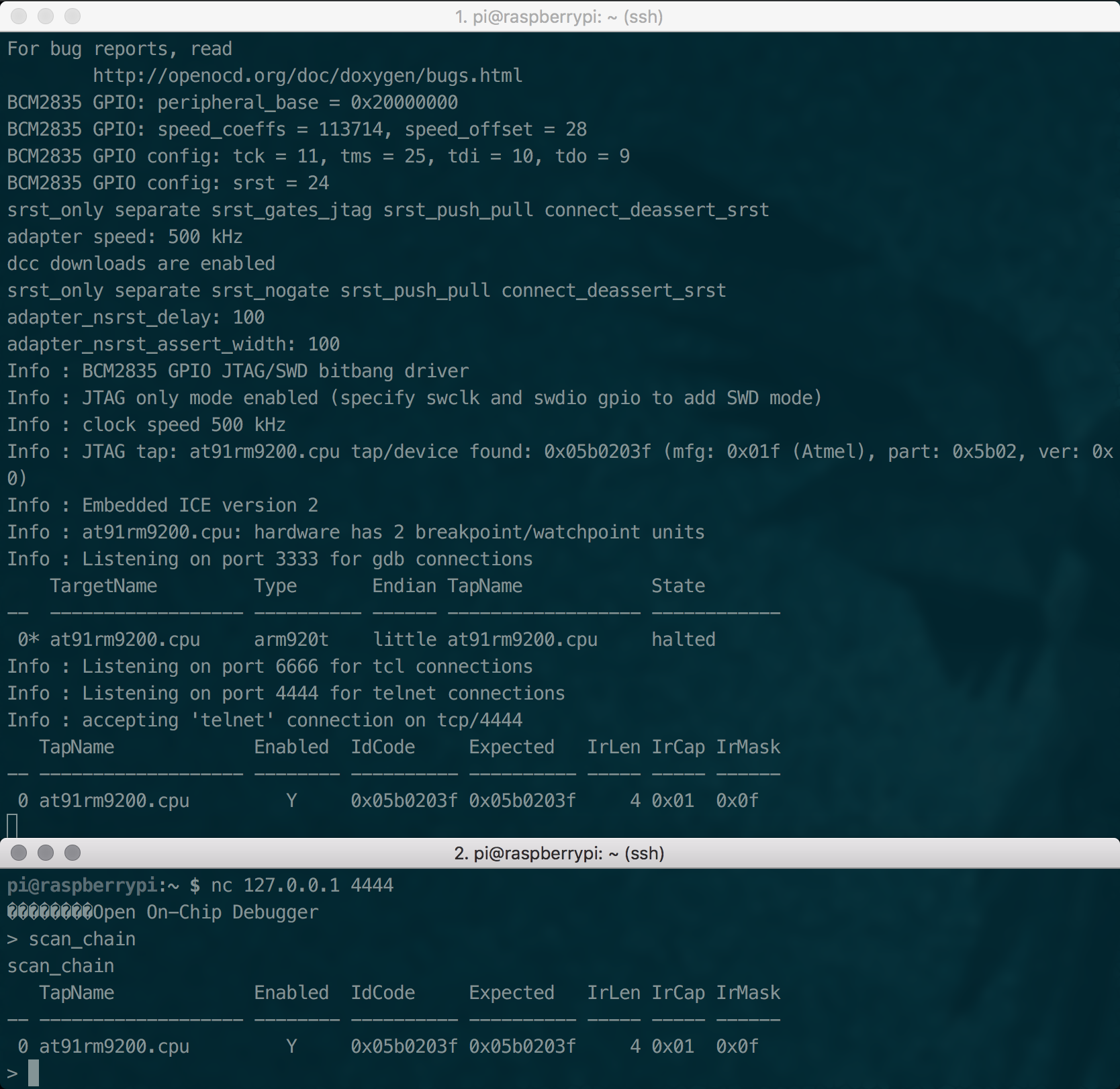
Figure 9: Interacting with the HMU through JTAG
Dumping the firmware Link to heading
OpenOCD provides us with a dump_image command which reads the memory. By using the memory map of the microcontroller presented in Figure 10, it is easy to dump specific blocks of memory. Sections of interest include the bootloader, the content of the flash memory and of the external flash memory. The corresponding addresses and size can be retrieved from the memory map in the datasheet (see Figure 10).
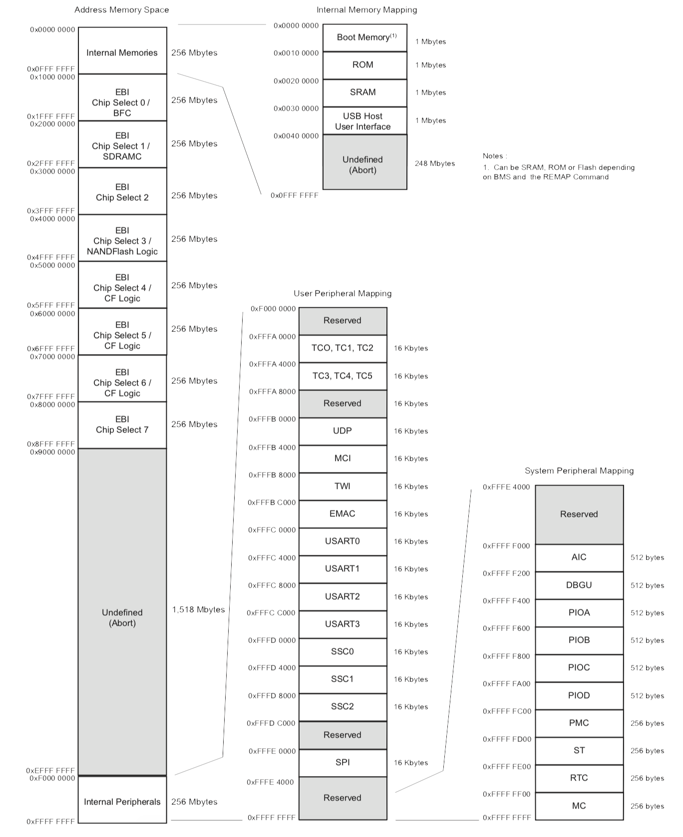
Figure 10: AT91RM9200 Memory map
To automatically dump the sections of the memory I was interested in, I used the following OpenOCD configuration file:
# INTERFACE
interface bcm2835gpio
bcm2835gpio_peripheral_base 0x20000000
bcm2835gpio_speed_coeffs 113714 28
bcm2835gpio_jtag_nums 11 25 10 9
bcm2835gpio_srst_num 24
reset_config srst_only srst_push_pull
adapter_khz 500

# TRANSPORT
transport select jtag

# TARGET
set WORKAREASIZE 0
set CHIPNAME at91rm9200
source [find target/at91rm9200.cfg]
reset_config srst_only srst_nogate
adapter_nsrst_delay 100
adapter_nsrst_assert_width 100

# EXEC
init
targets
halt

echo "Dumping bootloader..."
dump_image bootloader.img 0x00000000 1048576
echo "Done!"

echo "Dumping SRAM..."
dump_image sram.img 0x00200000 104576
echo "Done!"

echo "Dumping Flash content..."
dump_image flash.img 0x10000000 4194304
echo "Done!"

echo "Dumping RAM..."
dump_image sdram.img 0x20000000 2097152
echo "Done!"
This worked as a charm! Once connected to device, we can launch the “script”, and around 5 minutes later (I haven’t tried to speed up the process), we have our four memory dumps!
Conclusion Link to heading
To sum up, we put apart the device, figured out what the main components are and what are their capabilities. We then used that knowledge to determine the debug ports, even though they were not labelled. Finally, we dumped the memory of the device using the JTAG access and obtained the firmware of the HMU. In the next post, we will see how we can take advantage of the lack of mutual authentication between the device and the backend server to extract data out of it. In the fourth post, we will see how we can use the acquired firmware to reverse engineer the proprietary protocol used by the HMU to communicate with the backend server.
Go to Part 3 - Network Analysis of the HMU and Data Extraction.